Cadence Concept Schematic Capture Creating Schematic And Sym
Schematic capture eda pcb logical cadence circuit automation ema credit Pspice advanced analysis for parasitic capacitance Cadence schematic tutorial lab1 simulation capture lab shown
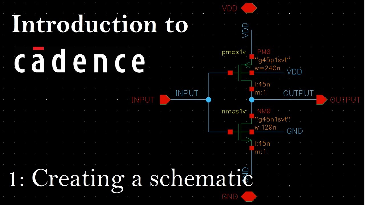
Intro to Cadence 1: Creating a Schematic and Symbol - YouTube
How to convert a cadence schematic image into white diagram Starting the schematics design in cadence schematic capture Schematic tutorial in cadence
Schematic capture with cadence pspice (2nd edition)
Lab/tutorial 1Pcb pro Creating schematic and symbol in cadence: a step-by-step guideSchematic capture and logical design.
How to convert a cadence schematic image into white diagramHow to take a screen capture for complete schematic view in batch mode Lab/tutorial 1Cadence schematic symbol virtuoso.

Can not change instance in schematic view
Intro to cadence 1: creating a schematic and symbolCadence schematic suite Cadence tutorial 1 from cmosedu.comFillable online cadence tutorial a: schematic entry and functional.
Cadence schematic captureLab/tutorial 1 Starting the schematics design in cadence schematic captureCadence schematic capture.
Simultaneous simulation of extracted and schematic views?
Circuit schematic in cadence design suiteLab1report2018.docx How to convert a cadence schematic image into white diagramCadence基础操作:schematic编辑_cadence界面拖动视图-csdn博客.
Cadence schematic to layoutCadence layout from schematic Circuit cadence lab1Cadence schematic tutorial command typing directory lab1 capture simulation lab pwd staring correct execute sure note start before make.

Starting the schematics design in cadence schematic capture
9780130276940: schematic capture with cadence pspiceQuickly view schematics, pcbs, and ic packages Cadence schematic tutorialStarting the schematics design in cadence schematic capture.
Cadence pcb viewers viewer schematic capture blogs community ic packages quickly boards using designs reorganized easily rich start useSchematic capture – attuned designs Starting the schematics design in cadence schematic capture.


